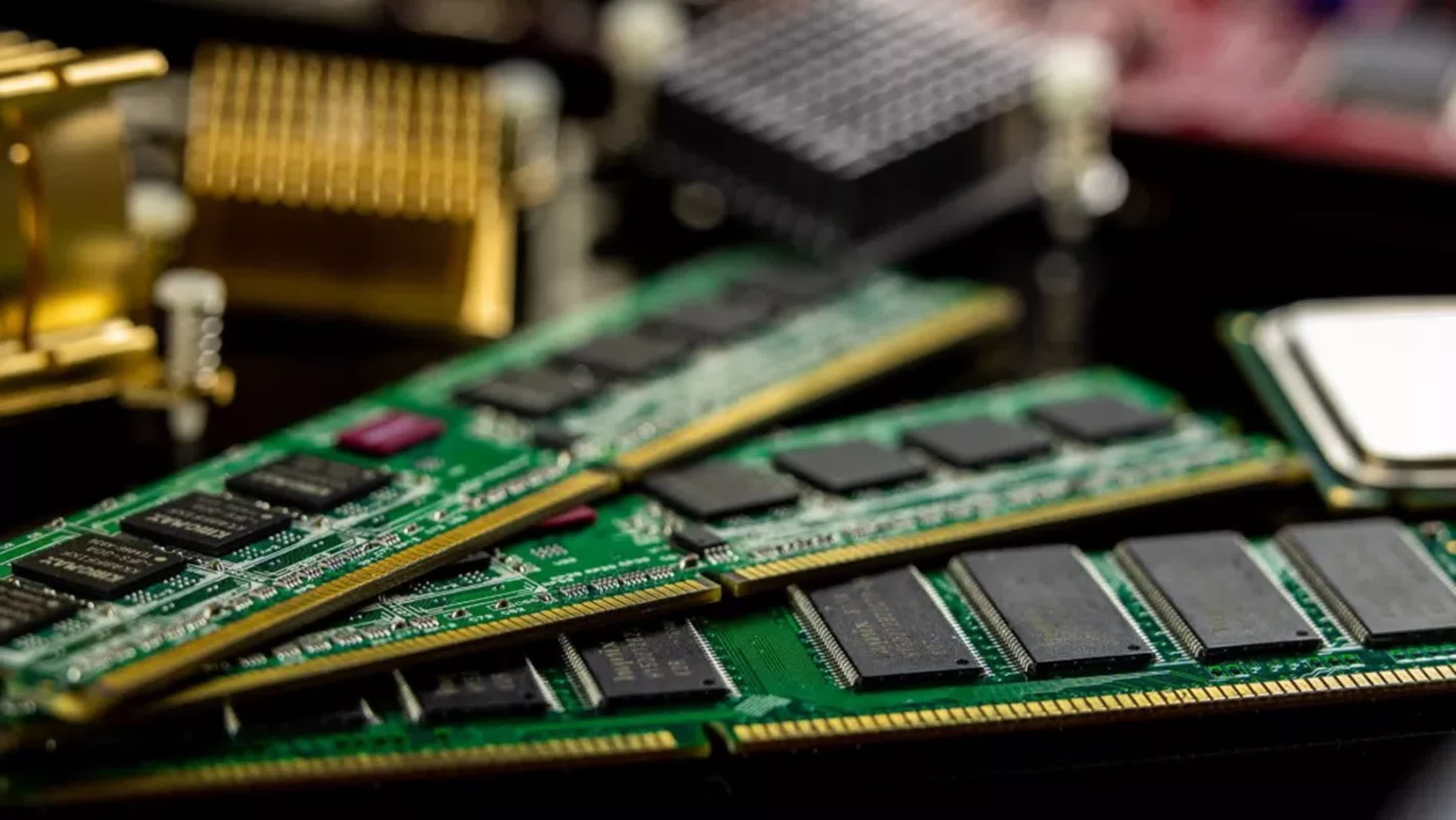
Something to look forward to: The memory industry is known for its conservative approach, often favoring incremental improvements over revolutionary changes. But as we look toward the end of the decade, it seems likely that the world will see the emergence of 3D monolithic stacked DRAM. The only questions that remain are what form it will take and when it will be ready for mass production.
While flash memory has made significant strides in capacity through monolithic 3D processing, DRAM has faced challenges in achieving a similar 3D architecture. The primary obstacle has been the need for a sufficiently large means of storing charge, typically in the form of a capacitor. The most straightforward approach to increasing data storage on a single-layer DRAM chip is to reduce the cell size.

However, the vertical capacitor in traditional DRAM designs creates very thick layers, making stacking difficult. To address this, some efforts are focused on running the capacitors horizontally, while others aim to eliminate the capacitor altogether. "DRAM is following in the steps of NAND by evolving to three dimensions in order to build more storage per unit area," said Benjamin Vincent, worldwide senior manager of semiconductor process and integration at Lam Research.
"This is good for the industry because it pushes the technological envelope for memory, and because more bits per square micrometer mean production costs decrease." It's important to note that 3D DRAM can refer to two distinct concepts. One already in production is High-Bandwidth Memory (HBM).
However, HBM is a stacked-die memory, not a monolithic die like 3D NAND flash. The development of a monolithic 3D DRAM chip could provide an immediate boost if employed in the HBM architecture, Daryl Seitzer, principal product manager for embedded memories at Synopsys, told Semiconductor Engineering. "When commercially viable 3D DRAM is available and die stacking challenges such as thermal management have been further addressed, this would be good news for HBM providers as it introduces memory density and energy efficiency improvements that will be impactful for data center and AI applications," he said.
One approach to optimizing DRAM cells involves shrinking feature sizes through advanced lithography techniques. The most recent steps toward footprint reduction pit EUV patterning against traditional ArF SADP and SAQP processes for cutting-edge 2D DRAM, according to Daniel Soden, business development manager at Brewer Science. Samsung is working on a new cell architecture that aims to achieve an area efficiency of 4F2 (where F is the minimum feature size).
This design employs a vertical-channel transistor and moves from the current 6F2 cell to 4F2. However, it will require new materials, including ferroelectrics, and high precision to build. Another promising direction involves laying the capacitor on its side to create thinner layers suitable for stacking.
Lam Research has proposed several ideas for achieving this, including flipping the cell, sliding the bit line, and employing gate-all-around (GAA) transistors. "Etch and deposition experts may be shocked at what our simulations propose," Vincent said. "For example, trenches with 30nm critical dimensions and 2μm depth are considered to be etched and filled in our architecture.
" Researchers are also exploring capacitor-less DRAM designs. One alternative involves gate-controlled thyristors, while another employs a floating body similar to the floating gate used in flash memory. Neo Semiconductor has proposed a commercial technology using a floating-body cell with dual gating.
"Based on simulations, this mechanism can increase the sensing margin and data retention," Andy Hsu, CEO and co-founder of Neo Semiconductor, said. While these advancements are promising, it's important to note that 3D DRAM is not just around the corner. All current efforts will require many years of development and evaluation before they have commercial traction.
"New architectures are always more challenging than implementation of existing methodologies," Soden said..


